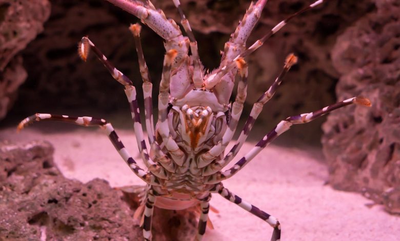
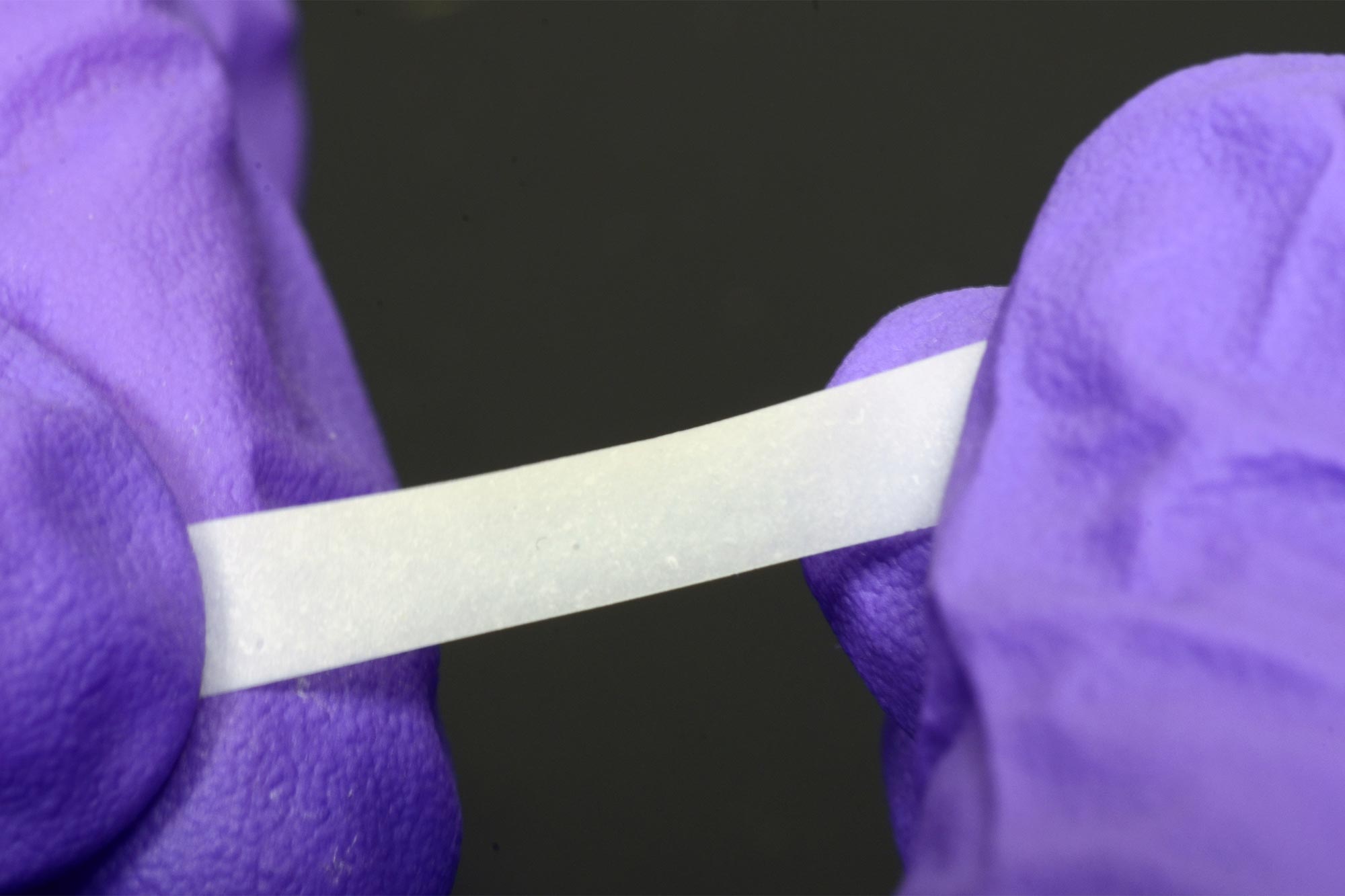
Lead image: An MIT team has fabricated a hydrogel-based material that mimics the structure of the lobster’s underbelly, the toughest known hydrogel found in nature.
The membrane’s structure could provide a blueprint for robust artificial tissues.
A lobster’s underbelly is lined with a thin, translucent membrane that is both stretchy and surprisingly tough. This marine under-armor, as MIT engineers reported in 2019, is made from the toughest known hydrogel in nature, which also happens to be highly flexible. This combination of strength and stretch helps shield a lobster as it scrabbles across the seafloor, while also allowing it to flex back and forth to swim.
Now a separate MIT team has fabricated a hydrogel-based material that mimics the structure of the lobster’s underbelly. The researchers ran the material through a battery of stretch and impact tests, and showed that, similar to the lobster underbelly, the synthetic material is remarkably “fatigue-resistant,” able to withstand repeated stretches and strains without tearing.
If the fabrication process could be significantly scaled up, materials made from nanofibrous hydrogels could be used to make stretchy and strong replacement tissues such as artificial tendons and ligaments.
The team’s results were recently published in the journal Matter. The paper’s MIT co-authors include postdocs Jiahua Ni and Shaoting Lin; graduate students Xinyue Liu and Yuchen Sun; professor of aeronautics and astronautics Raul Radovitzky; professor of chemistry Keith Nelson; mechanical engineering professor Xuanhe Zhao; and former research scientist David Veysset PhD ’16, now at Stanford University; along with Zhao Qin, assistant professor at Syracuse University, and Alex Hsieh of the Army Research Laboratory.
Nature’s twist
In 2019, Lin and other members of Zhao’s group developed a new kind of fatigue-resistant material made from hydrogel — a gelatin-like class of materials made primarily of water and cross-linked polymers. They fabricated the material from ultrathin fibers of hydrogel, which aligned like many strands of gathered straw when the material was repeatedly stretched. This workout also happened to increase the hydrogel’s fatigue resistance.
“At that moment, we had a feeling nanofibers in hydrogels were important, and hoped to manipulate the fibril structures so that we could optimize fatigue resistance,” says Lin.
In their new study, the researchers combined a number of techniques to create stronger hydrogel nanofibers. The process starts with electrospinning, a fiber production technique that uses electric charges to draw ultrathin threads out of polymer solutions. The team used high-voltage charges to spin nanofibers from a polymer solution, to form a flat film of nanofibers, each measuring about 800 nanometers — a fraction of the diameter of a human hair.
They placed the film in a high-humidity chamber to weld the individual fibers into a sturdy, interconnected network, and then set the film in an incubator to crystallize the individual nanofibers at high temperatures, further strengthening the material.
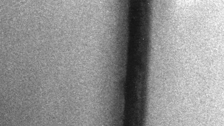
They tested the film’s fatigue-resistance by placing it in a machine that stretched it repeatedly over tens of thousands of cycles. They also made notches in some films and observed how the cracks propagated as the films were stretched repeatedly. From these tests, they calculated that the nanofibrous films were 50 times more fatigue-resistant than the conventional nanofibrous hydrogels.
Around this time, they read with interest a study by Ming Guo, associate professor of mechanical engineering at MIT, who characterized the mechanical properties of a lobster’s underbelly. This protective membrane is made from thin sheets of chitin, a natural, fibrous material that is similar in makeup to the group’s hydrogel nanofibers.
Guo found that a cross-section of the lobster membrane revealed sheets of chitin stacked at 36-degree angles, similar to twisted plywood, or a spiral staircase. This rotating, layered configuration, known as a bouligand structure, enhanced the membrane’s properties of stretch and strength.
“We learned that this bouligand structure in the lobster underbelly has high mechanical performance, which motivated us to see if we could reproduce such structures in synthetic materials,” Lin says.
Angled architecture
Ni, Lin, and members of Zhao’s group teamed up with Nelson’s lab and Radovitzky’s group in MIT’s Institute for Soldier Nanotechnologies, and Qin’s lab at Syracuse University, to see if they could reproduce the lobster’s bouligand membrane structure using their synthetic, fatigue-resistant films.
“We prepared aligned nanofibers by electrospinning to mimic the chinic fibers existed in the lobster underbelly,” Ni says.
After electrospinning nanofibrous films, the researchers stacked each of five films in successive, 36-degree angles to form a single bouligand structure, which they then welded and crystallized to fortify the material. The final product measured 9 square centimeters and about 30 to 40 microns thick — about the size of a small piece of Scotch tape.
Stretch tests showed that the lobster-inspired material performed similarly to its natural counterpart, able to stretch repeatedly while resisting tears and cracks — a fatigue-resistance Lin attributes to the structure’s angled architecture.
“Intuitively, once a crack in the material propagates through one layer, it’s impeded by adjacent layers, where fibers are aligned at different angles,” Lin explains.
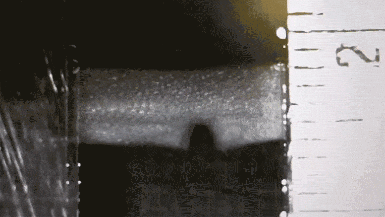
The team also subjected the material to microballistic impact tests with an experiment designed by Nelson’s group. They imaged the material as they shot it with microparticles at high velocity, and measured the particles’ speed before and after tearing through the material. The difference in velocity gave them a direct measurement of the material’s impact resistance, or the amount of energy it can absorb, which turned out to be a surprisingly tough 40 kilojoules per kilogram. This number is measured in the hydrated state.
It’s no surprise that the new material isn’t as tough as commercial antiballistic materials. It is, however, significantly sturdier than most other nanofibrous hydrogels such as gelatin and synthetic polymers like PVA. The material is also much stretchier than Kevlar. This combination of stretch and strength suggests that, if their fabrication can be sped up, and more films stacked in bouligand structures, nanofibrous hydrogels may serve as flexible and tough artificial tissues.
“For a hydrogel material to be a load-bearing artificial tissue, both strength and deformability are required,” Lin says. “Our material design could achieve these two properties.”
Reference: “Strong fatigue-resistant nanofibrous hydrogels inspired by lobster underbelly” by Jiahua Ni, Shaoting Lin, Zhao Qin, David Veysset, Xinyue Liu, Yuchen Sun, Alex J. Hsieh, Raul Radovitzky, Keith A. Nelson and Xuanhe Zhao, 23 April 2021, Matter.
DOI: 10.1016/j.matt.2021.03.023
This research was supported, in part, by MIT and the U. S. Army Research Office through the Institute for Soldier Nanotechnologies at MIT.