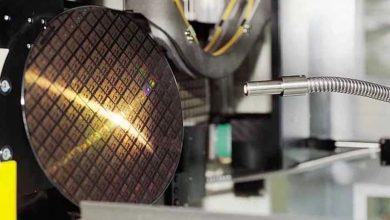
A while back, TSMC had stated that they won’t be building a production facility in the US, but apparently, they went back against their previous statement, and decided to start manufacturing in the US in another statement. TSMC officially announced that they will be building a new high end fabrication plant in Arizona. The fabrication plant will be fabricating 5nm process nodes for most electronic companies that needs them for processors, graphics cards and the like. The new fab will have the capacity to produce around 20,000 wafers per month. The entire building will be costing a whopping $12 billion.
US Pressure
TSMC serves the US and China, 2 countries who are in economic conflict with each other. This caused TSMC to be caught in the crossfire. The US has pressured TSMC into building a plant in America, and TSMC bowed in. While China has been reliant on TSMC’s fabs, the US does too, since GlobalFoundries retreated, and thus TSMC decided to cave in, and start a factory in the US. This is going to be the first time when TSMC makes a cutting-edge manufacturing fab outside Taiwan.
3nm at Arizona plant
Currently, the 5 nanometer manufacturing process is currently the most advanced process, and will be first seen in Apple’s chips on the iPhone 12. But by the time the Arizona plant is built up, TSMC will already be on the way to producing 3nm, and would make the Arizona facility the most advanced fab manufacturing facility, and also the most advanced contract fab in the United States.
Other US fabs
The chip fab won’t be TSMC’s first facility or even chip fab in the U.S. either. The company operates design centers in Austin, Texas, and San Jose, California, as well as a smaller chip fab in Camas, Washington.. But the difference between the two fabs is that the one in Washington builds fabs on process nodes of 350 to 160nm, while the new one in Arizona will be building fabs on 3nm. The Camas fab is making fabs for flash storage, and thus uses those relatively large process nodes. Thus the Arizona fab is one of the best, most advanced fab compared to the others.
Arizona Fab
The Arizona fab is touted as a medium sized facility even though it’s being the most advanced manufacturing node. The fab can produce just 20,000 wafers monthly, compared to the “Gigafabs” fab back home in Taiwan which can produce a fab of 100,000 wafers monthly. So, while the fab will be using TSMC’s latest process node at the time, it won’t have a massive capacity. But with that 12 billion dollar price tag, it would definitely be the most expensive building from TSMC
TSMC aims to begin construction on the project in 2021 with a completion date targeted for some time in 2024.
“This project is of critical, strategic importance to a vibrant and competitive U.S. semiconductor ecosystem that enables leading U.S. companies to fabricate their cutting-edge semiconductor products within the United States and benefit from the proximity of a world-class semiconductor foundry and ecosystem,” the company said in a statement.
While this will expand TSMC’s presence in the U.S., The Wall Street Journal reports that even at full capacity the proposed facility would be a drop in the bucket compared to the 12 million wafers it produced last year.
A victory for Trump, but may not be so much for America
President Donald Trump has an “America-first” agenda, and thus getting TSMC to start a plant in the US sounded like a victory so that it would help bring manufacturing back home. But while it might look all fine and dandy, the reality is different. Many analysts warned that the US companies could see a revenue decline of around 37% if the US were to completely ban semiconductor companies from selling to Chinese customers, in effect causing a “technology decoupling” from China. That would actually be disastrous for the US.
TSMC’s goals
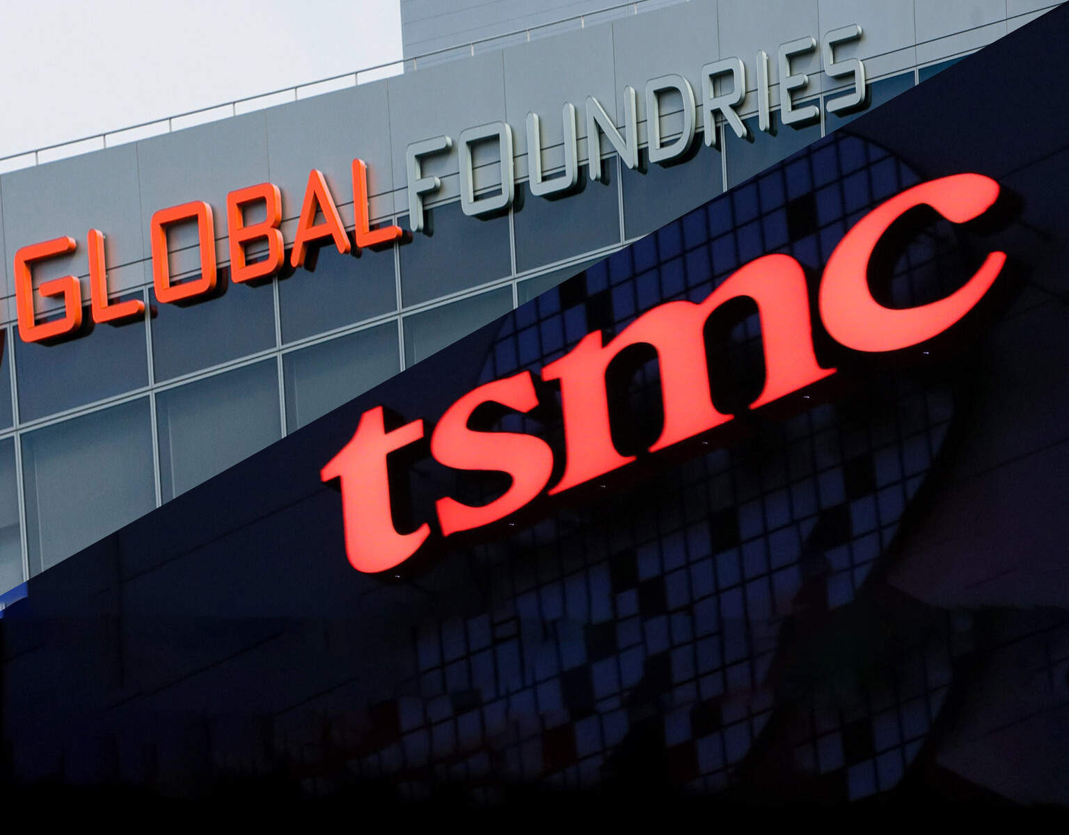
The primary reason for building the fab in the US rather than in Taiwan is to have a high end production capacity inside the United States. According to a report by Reuters, Globalfoundries is dropping out of the semiconductor race(to build the smallest node) and will instead concentrate on refining it’s existing nodes. So while Globalfoundries is heading out, the US is in need of a fabrication with a leading edge facility to be present in the US for building their chips, and TSMC is the best candidate for the job.
Domestic fabs currently in the US
It may be no surprise as the current domestic fabs present in the US – Intel, and Globalfoundries are looking at this deal with a dreaded look on their face. Intel has been trying to lure customers to it’s contract manufacturing business, but with little to no luck. Globalfoundries on the other hand is the US’s main fab for the military. Globalfoundries inherited the business from IBM, but now face a threat as the US government will want to switch to newer manufacturing processes, and will use the outsider’s, TSMC rather than their own.
After starting the building of the fabrication in 2021, and subsequent completion in 2024, TSMC will employ around 1,600 workers, and will be the second leading edge foundry provider for the United States.

