Lead Image: Hubble has used microlensing to measure the mass of a white dwarf star.
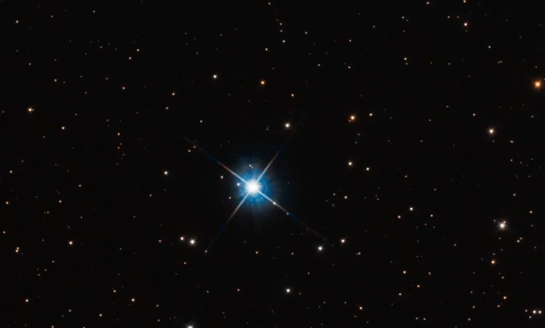
The dwarf, called LAWD 37, is a burned-out star in the center of this NASA/ESA Hubble Space Telescope image. Though its nuclear fusion furnace has shut down, trapped heat is sizzling on the surface at roughly 100 000 degrees Celsius, causing the stellar remnant to glow fiercely.
The white dwarf has a ‘spike’ because it is so bright that the light ‘bled’ into the Hubble camera’s CCD detector. This interfered with one of the observing dates for measuring that background star’s position on the sky.
Credit: NASA, ESA, P. McGill (Univ. of California, Santa Cruz and University of Cambridge), K. Sahu (STScI), J. Depasquale (STScI)
Astronomers using the NASA/ESA Hubble Space Telescope have for the first time directly measured the mass of a single, isolated white dwarf star – the surviving core of a burned-out sunlike star.
Researchers found that the white dwarf is 56 percent of the mass of our Sun. This agrees with earlier theoretical predictions of its mass and corroborates current theories of how white dwarfs evolve as the end product of a typical star’s evolution. The unique observation yields insights into theories of the structure and composition of white dwarfs.
Until now, previous white dwarf mass measurements have been gleaned from observing white dwarfs in binary star systems. By watching the motion of two co-orbiting stars, straightforward Newtonian physics can be used to measure their masses. However, these measurements can be uncertain if the dwarf’s companion star is in a long-period orbit of hundreds or thousands of years. Orbital motion can be measured by telescopes only over a brief slice of the dwarf’s orbital motion.
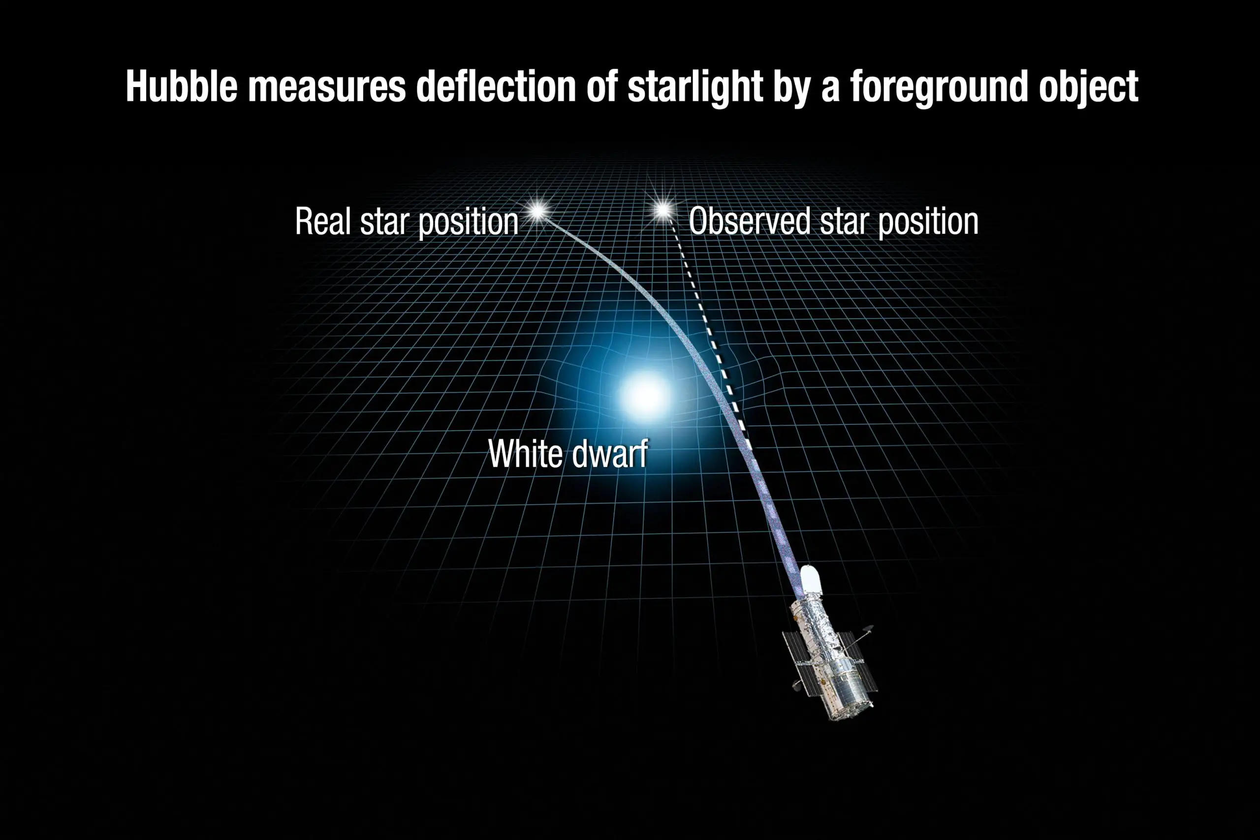
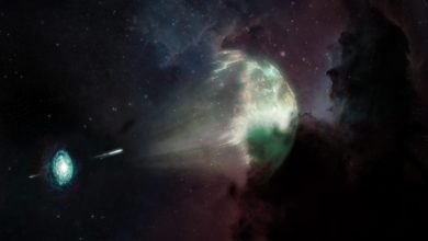
This effect, called gravitational lensing, was predicted as a consequence of Einstein’s general theory of relativity from a century ago. Observations of a solar eclipse in 1919 provided the first experimental proof for general relativity. But Einstein didn’t think the same experiment could be done for stars beyond our Sun because of the extraordinary precision required.
Credit: NASA, ESA, A. Feild
For this companion-less white dwarf, researchers had to employ a trick of nature, called gravitational microlensing. The light from a background star was slightly deflected by the gravitational warping of space by the foreground dwarf star. As the white dwarf passed in front of the background star, microlensing caused the star to appear temporarily offset from its actual position on the sky.
The results are reported in the journal Monthly Notices of the Royal Astronomical Society. The lead author is Peter McGill, formerly of the University of Cambridge in the United Kingdom and now based at the University of California, Santa Cruz.
McGill used Hubble to precisely measure how light from a distant star bent around the white dwarf, known as LAWD 37, causing the background star to temporarily change its apparent position in the sky.
Kailash Sahu of the Space Telescope Science Institute in Baltimore, Maryland, USA, the principal Hubble investigator on this latest observation, first used microlensing in 2017 to measure the mass of another white dwarf, Stein 2051 B. But that dwarf is in a widely separated binary system. “Our latest observation provides a new benchmark because LAWD 37 is all by itself,” Sahu said.
The collapsed remains of a star that burned out 1 billion years ago, LAWD 37 has been extensively studied because it is only 15 light-years away in the constellation Musca. “Because this white dwarf is relatively close to us, we’ve got lots of data on it — we’ve got information about its spectrum of light, but the missing piece of the puzzle has been a measurement of its mass,” said McGill.
The team zeroed-in on the white dwarf thanks to ESA’s Gaia mission, which makes extraordinarily precise measurements of nearly two billion star positions. Multiple Gaia observations can be used to track a star’s motion. Based on these data, astronomers were able to predict that LAWD 37 would briefly pass in front of a background star in November 2019.
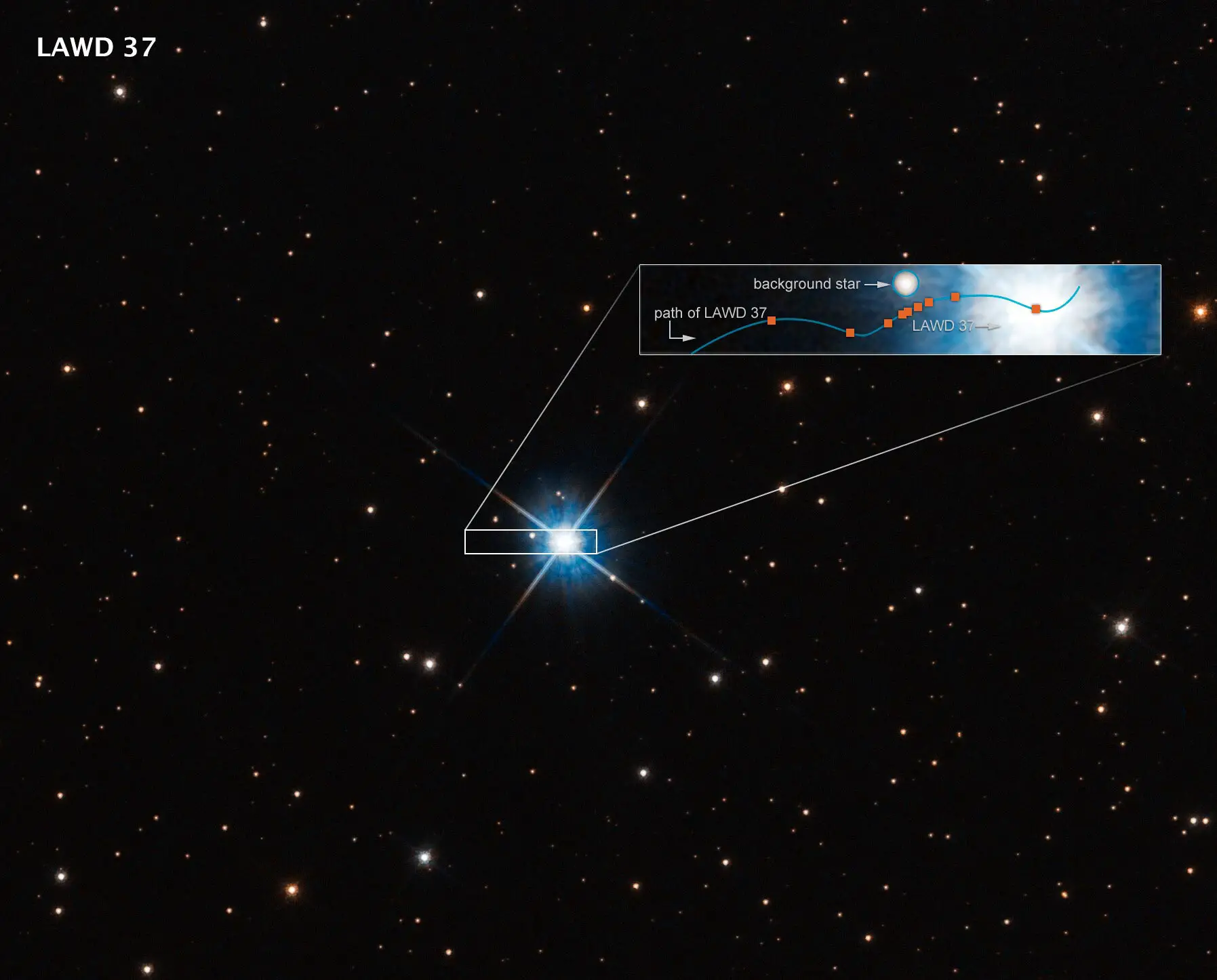
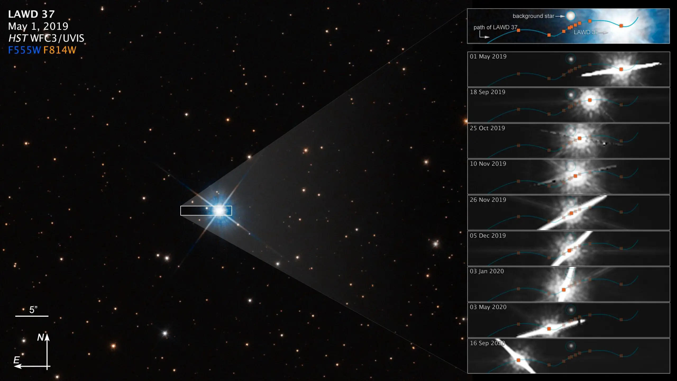
The dwarf, called LAWD 37, is a burned-out star in the center of this Hubble Space Telescope image. Though its nuclear fusion furnace has shut down, trapped heat is sizzling on the surface at roughly 100,000 degrees Celsius, causing the stellar remnant to glow fiercely.
The inset box plots how the dwarf passed in front of a background star in 2019. The wavy blue line traces the dwarf’s apparent motion across the sky as seen from Earth. Though the dwarf is following a straight trajectory, the motion of Earth as it orbits the Sun imparts an apparent sinusoidal offset due to parallax. (The star is only 15 light-years away. Therefore, it is moving at a faster rate against the stellar background.)
As it passed by the fainter background star, the dwarf’s gravitational field warped space (as Einstein’s general theory of relativity predicted a century ago). And this deflection was precisely measured by Hubble’s extraordinary resolution. The amount of deflection yields a mass for the white dwarf of 56 percent of our Sun’s mass and provides insights into theories of the structure and composition of white dwarfs. This is the first time astronomers have directly measured the mass of a single, isolated star other than our Sun.
Credit: NASA, ESA, P. McGill (Univ. of California, Santa Cruz and Univ. of Cambridge), K. Sahu (STScI), J. Depasquale (STScI)
Once this was known, Hubble was used to precisely measure over several years how the background star’s apparent position in the sky was temporarily deflected during the white dwarf’s passage.
“These events are rare, and the effects are tiny,” said McGill. “For instance, the size of our measured offset is like measuring the length of a car on the Moon as seen from Earth.”
Since the light from the background star was so faint, the main challenge for astronomers was extracting its image from the glare of the white dwarf, which is 400 times brighter than the background star. Only Hubble can make these kinds of high-contrast observations in visible light.
The dwarf, called LAWD 37, is a burned-out star in the center of this Hubble Space Telescope image. Though its nuclear fusion furnace has shut down, trapped heat is sizzling on the surface at roughly 100,000 degrees Celsius, causing the stellar remnant to glow fiercely.
The inset boxes at right plot how the dwarf passed in front of a background star in 2019. The wavy blue line traces the dwarf’s apparent motion across the sky as seen from Earth. Though the dwarf is following a straight trajectory, the motion of Earth as it orbits the Sun imparts an apparent sinusoidal offset due to parallax. (The star is only 15 light-years away, and therefore is moving at a faster rate against the stellar background.)
As it passed by the fainter background star, the dwarf’s gravitational field warped space (as Einstein’s general theory of relativity predicted a century ago). And this deflection was precisely measured by Hubble’s extraordinary resolution. The dwarf’s offset position is colored orange.
The amount of deflection yields a mass for the white dwarf of 56 percent of our Sun’s mass, and this provides insights into theories of the structure and composition of white dwarfs. This is the first time that astronomers have directly measured the mass of a single, isolated star other than our Sun.
The white dwarf has a ‘spike’ because it is so bright that the light ‘bled’ into the Hubble camera’s CCD detector. This interfered with one of the observing dates for measuring that background star’s position on the sky.
The compass graphic points to the object’s orientation on the celestial sphere. North points to the north celestial pole which is not a fixed point in the sky, but it currently lies near the star Polaris, in the circumpolar constellation Ursa Minor. Celestial coordinates are analogous to a terrestrial map, though east and west are transposed because we are looking up rather than down.
Credit: NASA, ESA, P. McGill (Univ. of California, Santa Cruz and University of Cambridge), K. Sahu (STScI), J. Depasquale (STScI)
“Even when you’ve identified such a one-in-a-million event, it’s still extremely difficult to make these measurements,” said Leigh Smith of the University of Cambridge. “The glare from the white dwarf can cause streaks in unpredictable directions, meaning we had to analyze each of Hubble’s observations extremely carefully, and their limitations, to model the event and estimate the mass of LAWD 37.”
“The precision of LAWD 37’s mass measurement allows us to test the mass-radius relationship for white dwarfs,” said McGill. “This means testing the theory of degenerate matter (a gas so super-compressed under gravity that it behaves more like solid matter) under the extreme conditions inside this dead star,” he added.
The researchers say their results open the door for future event predictions with Gaia data. In addition to Hubble, these alignments can now be detected with the NASA/ESA/CSA James Webb Space Telescope. Because Webb works at infrared wavelengths, the blue glow of a foreground white dwarf looks dimmer in infrared light, and the background star looks brighter.
Hubble has used microlensing to measure the mass of a white dwarf star.
The dwarf, called LAWD 37, is a burned-out star in the center of this Hubble Space Telescope image that is featured in this pan video. Though its nuclear fusion furnace has shut down, trapped heat is sizzling on the surface at roughly 100,000 degrees Celsius, causing the stellar remnant to glow fiercely.
The white dwarf has a ‘spike’ because it is so bright that the light ‘bled’ into the Hubble camera’s CCD detector. This interfered with one of the observing dates for measuring that background star’s position on the sky.
Credit: NASA, ESA, P. McGill (Univ. of California, Santa Cruz and University of Cambridge), K. Sahu (STScI), J. Depasquale (STScI), N. Bartmann (ESA/Webb)
Music: Mylonite – Breath of my Soul
Based on Gaia’s predictive powers, Sahu is observing another white dwarf, LAWD 66, with Webb. The first observation was made in 2022. More observations will be taken as the deflection peaks in 2024 and then subsides.
“Gaia has really changed the game — it’s exciting to be able to use Gaia data to predict when events will happen, and then observe them happening,” said McGill. “We want to continue measuring the gravitational microlensing effect and obtain mass measurements for many more types of stars.”
In his 1915 general theory of relativity, Einstein predicted that when a massive compact object passes in front of a background star, the light from the star would bend around the foreground object because of the warping of space by its gravitational field.
Exactly a century before this latest Hubble observation, in 1919, two British-organised expeditions to the southern hemisphere first detected this lensing effect during a solar eclipse on 19 May. It was hailed as the first experimental proof of general relativity — that gravity warps space. However, Einstein was pessimistic that the effect could ever be detected for stars outside our Solar System because of the precision required. “Our measurement is 625 times smaller than the effect measured at the 1919 solar eclipse,” said McGill.
More information
The Hubble Space Telescope is a project of international cooperation between ESA and NASA.
The international team of astronomers in this study consists of Peter McGill (University of Cambridge, UK; University of California Santa Cruz, USA), Jay Anderson (Space Telescope Science Institute, USA), Stefano Casertano (Space Telescope Science Institute, USA), Kailash C. Sahu (Space Telescope Science Institute, USA), Pierre Bergeron (University of Montreal, Canada), Simon Blouin (University of Victoria, Canada), Patrick Dufour (University of Montreal, Canada), Leigh C. Smith (University of Cambridge, UK), N. Wyn Evans (University of Cambridge, UK), Vasily Belokurov (University of Cambridge, UK), Richard L. Smart (INAF – Astrophysical Observatory of Torino, Italy), Andrea Bellini (Space Telescope Science Institute, USA), Annalisa Calamida (Space Telescope Science Institute, USA), Martin Dominik (University of St Andrews, UK), Noé Kains (Space Telescope Science Institute, USA), Jonas Klüter (Louisiana State University, USA), Martin Bo Nielsen (University of Birmingham, UK; Aarhus University, Denmark; New York University Abu Dhabi, United Arab Emirates), and Joachim Wambsganss (Heidelberg University, Germany)