There are conflicting reports on which Apple iPhone will get mmWave 5G version. Some say that Only the Pro variants would feature it. While others say that the mmWave variant will only be available for certain markets. That’s pretty confusing to be honest.
iPhone 12 mmWave delay
So what happened is, there’s a delay of 2 months in releasing the iPhone 12 with mmWave 5G. Most of it is credited to the pandemic. The current estimates are a few million units lower than expected. Apple was supposed to release at least 30 to 40 million units of iPhones with mmWave, but they have scaled down to 15 – 20 million units for the rest of 2020. Thus suppliers of AiP (Antenna in Package) are having intense competition, in reports by DigiTimes.
DigiTimes says that Apple’s AiP is more cost effective, compared to earlier designs. A few manufacturers have stated that the models with mmWave 5G will launch only after the ones with sub-6GHz are launched. They too have credited it to the pandemic. Thus, for countering these challenges, Apple decided to diversify their business, and keep the modules separate.
The upcoming mmWave 5G iPhones will adopt more cost-effective FC-AiP process, with ASE Technology to package AiP modules, the sources said. But Apple reportedly has finalized three suppliers of BT-based FC-AiP substrates, including one based in Taiwan and two in South Korea, and they will together supply 30-50 million substrates, the sources said, adding one iPhone will require 2-3 AiP modules.
Difference between 5G standards
There are 2 main 5G standards. The first is Sub-6GHz and the other is mmWave.
As the name says, sub-6GHz uses radio signals in the frequency bands of 6GHz and below, hence the moniker “sub-6GHz”. 5G speeds in the sub-6GHz will be faster than 4G, mostly due to 5G’s capacity enhancements at the back-haul. The other thing that increases 5G speeds is the bandwidth. 5G bands use a bandwidth of 100MHz in a single band for both sub-6GHz and mmWave, while 4G on the other hand supports a bandwidth of just 20MHz. Combining say 5 frequencies of 20MHz(in 4G) to make a single 100MHz is like aggregating 5 bands on 5G! Thus using 100MHz in a single frequency band would increase the speed of a handset by 2 to 3 times! The handsets in the sub-6GHz bands also support 4×4 MIMO, and 256QAM.
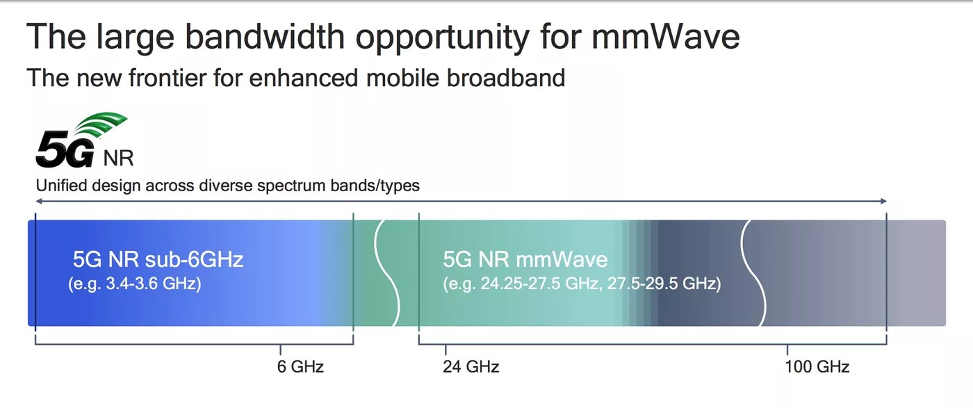
Coming to the mmWave, it’s termed as millimetre wave. The reason for that is, the radio wave is 1mm or more apart, hence the name mmWave. These waves are broad enough for high bandwidth needs, and support great speeds. The only drawback is that it’s unable to pass through objects like the ones in the sub-6GHz band. This is due to the density of the radio wave. They are really dense that even using your hand to block the signal could result in a significant signal loss. Handsets with millimeter waves support just 2×2 MIMO and 256QAM.
iPhone 5G variant launch
The reports say that the iPhone with sub-6GHz will launch earlier than expected, in about a month and a half, and will be widely available. This could mean that all models might feature the sub-6GHz iPhone, and would be available world over.
So, are you waiting for the new iPhones with 5G mmWave? Do let us know in the comments.