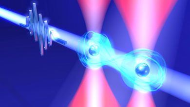
Lead Image: Physicists have created a remarkable, never-before-seen phase of matter in a quantum computer.
Physicists demonstrated a way of storing quantum information that is less prone to errors by subjecting a quantum computer’s qubits to quasi-rhythmic laser pulses based on the Fibonacci sequence.
Physicists have created a remarkable, never-before-seen phase of matter by shining a laser pulse sequence inspired by the Fibonacci sequence at atoms inside a quantum computer. Despite there still being only one singular flow of time, the phase has the benefits of two time dimensions, the physicists reported on July 20 in the journal Nature.
This mind-bending property offers a highly desirable benefit: Information stored in the phase is far more protected against errors than with alternative setups currently used in quantum computers. As a result, the information can exist for far longer without getting garbled, an important milestone for making quantum computing viable, according to study lead author Philipp Dumitrescu.
The approach’s innovative use of an “extra” time dimension “is a completely different way of thinking about phases of matter,” says Dumitrescu, who worked on the project as a research fellow at the Flatiron Institute’s Center for Computational Quantum Physics in New York City. “I’ve been working on these theory ideas for over five years, and seeing them come actually to be realized in experiments is exciting.”
Together with Andrew Potter of the University of British Columbia in Vancouver, Romain Vasseur of the University of Massachusetts, Amherst, and Ajesh Kumar of the University of Texas in Austin, Dumitrescu spearheaded the theoretical component of the research. A team headed by Brian Neyenhuis conducted the experiments on a quantum computer at Quantinuum in Broomfield, Colorado.
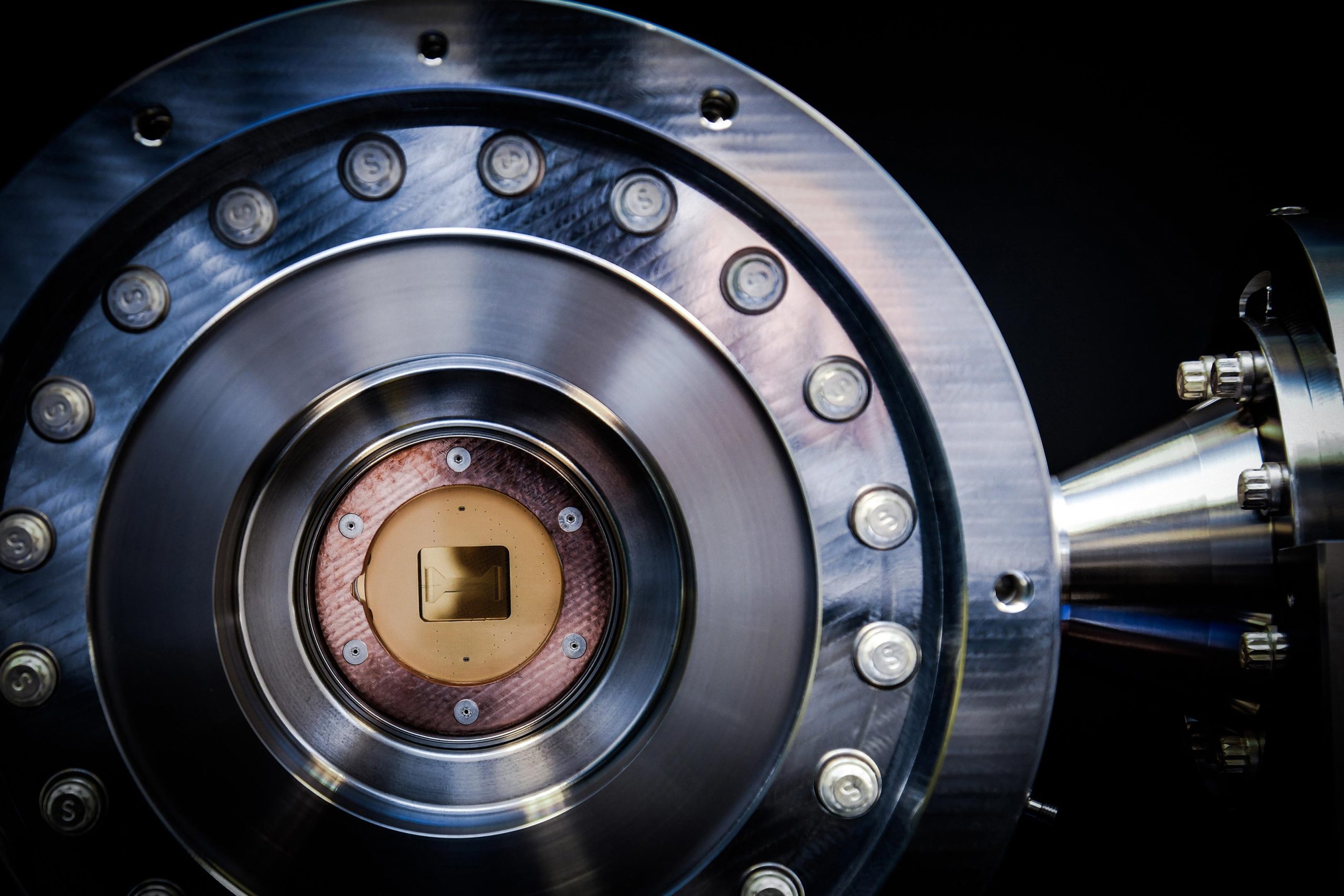
Ten atomic ions of the element ytterbium serve as the workhorses of the team’s quantum computer. Each ion is individually held and controlled by electric fields produced by an ion trap and can be manipulated or measured using laser pulses.
Each of those atomic ions function as what physicists dub a quantum bit, or ‘qubit.’ As opposed to conventional computers that quantify information in bits (each representing a 0 or a 1), the qubits used by quantum computers leverage the strangeness of quantum mechanics to store even more information. Just as Schrödinger’s cat is both dead and alive in its box, a qubit can be a 0, a 1, or a mashup — or ‘superposition’ — of both at the same time. That additional information density and the way qubits interact with one another promise to allow quantum computers to solve computational problems far beyond the reach of traditional computers.
However, there’s a big problem: Just as peeking in Schrödinger’s box seals the cat’s fate, so does interacting with a qubit. And that interaction doesn’t even have to be deliberate. “Even if you keep all the atoms under tight control, they can lose their quantumness by talking to their environment, heating up or interacting with things in ways you didn’t plan,” Dumitrescu says. “In practice, experimental devices have many sources of error that can degrade coherence after just a few laser pulses.”
Therefore, the challenge is to make qubits more robust. To do that, physicists can use ‘symmetries,’ which are essentially properties that hold up to change. (For example, a snowflake has rotational symmetry because it looks the same when rotated by 60 degrees.) One method is adding time symmetry by blasting the atoms with rhythmic laser pulses. This approach helps, but Dumitrescu and his collaborators wondered if they could go further. So instead of just one time symmetry, they aimed to add two by using ordered but non-repeating laser pulses.
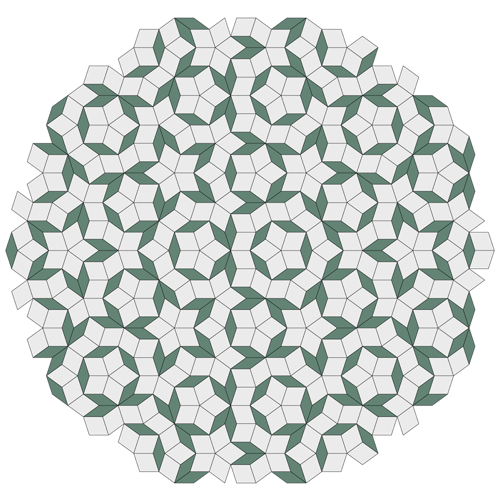
The best way to understand their approach is by considering something else ordered yet non-repeating: ‘quasicrystals.’ A typical crystal has a regular, repeating structure, like the hexagons in a honeycomb. A quasicrystal still has order, but its patterns never repeat. (Penrose tiling is one example of this.) Even more mind-boggling is that quasicrystals are crystals from higher dimensions projected, or squished down, into lower dimensions. Those higher dimensions can even be beyond physical space’s three dimensions: A 2D Penrose tiling, for instance, is a projected slice of a 5D lattice.
For the qubits, Dumitrescu, Vasseur, and Potter proposed in 2018 the creation of a quasicrystal in time rather than space. Whereas a periodic laser pulse would alternate (A, B, A, B, A, B, etc.), the researchers created a quasi-periodic laser-pulse regimen based on the Fibonacci sequence. In such a sequence, each part of the sequence is the sum of the two previous parts (A, AB, ABA, ABAAB, ABAABABA, etc.). This arrangement, just like a quasicrystal, is ordered without repeating. And, akin to a quasicrystal, it’s a 2D pattern squashed into a single dimension. That dimensional flattening theoretically results in two time symmetries instead of just one: The system essentially gets a bonus symmetry from a nonexistent extra time dimension.
Actual quantum computers are incredibly complex experimental systems, though, so whether the benefits promised by the theory would endure in real-world qubits remained unproven.
Using Quantinuum’s quantum computer, the experientialists put the theory to the test. They pulsed laser light at the computer’s qubits both periodically and using the sequence based on the Fibonacci numbers. The focus was on the qubits at either end of the 10-atom lineup; that’s where the researchers expected to see the new phase of matter experiencing two time symmetries at once. In the periodic test, the edge qubits stayed quantum for around 1.5 seconds — already an impressive length given that the qubits were interacting strongly with one another. With the quasi-periodic pattern, the qubits stayed quantum for the entire length of the experiment, about 5.5 seconds. That’s because the extra time symmetry provided more protection, Dumitrescu says.
“With this quasi-periodic sequence, there’s a complicated evolution that cancels out all the errors that live on the edge,” he says. “Because of that, the edge stays quantum-mechanically coherent much, much longer than you’d expect.”
Though the findings demonstrate that the new phase of matter can act as long-term quantum information storage, the researchers still need to functionally integrate the phase with the computational side of quantum computing. “We have this direct, tantalizing application, but we need to find a way to hook it into the calculations,” Dumitrescu says. “That’s an open problem we’re working on.”
Reference: “Dynamical topological phase realized in a trapped-ion quantum simulator” by Philipp T. Dumitrescu, Justin G. Bohnet, John P. Gaebler, Aaron Hankin, David Hayes, Ajesh Kumar, Brian Neyenhuis, Romain Vasseur and Andrew C. Potter, 20 July 2022, Nature.
DOI: 10.1038/s41586-022-04853-4